0 com

Italian night out!

To celebrate our group Christmas dinner in an Italian restaurant!


Fantastic pasta, secret family recipe: Cr + Au + HF etching!
0 com

graphene transistor

Hello everyone!

As I was browsing the scientific web today I came across this really nice review of graphene transistors. For everyone who would like to know more about this new invention the link here

The reasons to read it, one by one:

1. It's FOR FREE! (the article, not the transistor)
2. It's in Nature Nano, the best of nano journals
3. graphene transistors are the future of our electronics (or at least we like to believe that..)

Of course some of you may find it too long and too complicated, still it's worth to at least check out the pics ;)

And soon some of MY graphene transistors!
3 com

Salamandra


Feeling a bit fed up with those black-and-white SEM images, today it's time to color up!!!

I'm not so sure if anyone else sees a salamandra in this pic (I do!), in fact it's a leftover of the PMMA layer.
PMMA  is a special kind of resist which we use for electron beam lithography. In this resist we can 'draw' shapes and lines with the electron beam and then fill them with metal, so they stay forever on the chip (like the small cross in the left corner of the pic). The PMMA should go away with acetone, but sometimes it leaves some stains and residues, just like on this sample.


UPDATE! Since nobody else sees a salamandra I propose baboso del mar  (or a sea pancake!)
No. 3 on the list http://de10.com.mx/13048.html  :)
4 com

Silicon Fan


To mark our silicon chips we make a scratch with a diamond tip. Then in the region of the scratch we can sometimes find some pretty structures, just like this one. It reminds a little bit of a Spanish fan, the typical female accessory here, even in 21st century!
4 com

The high frequency resonator finally published!

figureThe good news from last week: the resonator paper is now available online here !


In the paper we measure vibrations of  a very short nanontube, which oscillates with very high frequency - up to 4.2 GHz! That's one of the highest frequencies up to now.


1 com

A bit more about CNT resonators...

Here I show you the image of a high-frequency CNT resonator. It's a suspended SWNT of 100nm length and 4nm diameter.


Now the explication :)
It operates in transistor geometry, as shown below. Source-drain is where the AC current flows, inducing vibrations and with changing voltage on the gate we can change nanotube mechanical tension.
And yes - the actual resonator is the ultra-short carbon nanotube! It's so tiny that it's difficult to image it in SEM. But because it's so small it's easy to achieve high frequency operation!


The details of the high frequency devices will be published in Applied Physics Letters SOON!!! But I'll also try to explain it here in an easier way!
0 com

Carbon nanotube resonators

During this year I worked a on mechanical resonators made of carbon nanotubes.

In general we have two types of carbon nanotubes (CNTs): single-walled (SWNT) and multi-walled (MWNT).  I also put the pictures, for those  who never got the chance to see them before. As the name suggests they are simply very little tubes, but their big advantage for mechanics and electronics is that they are very robust (the most robust material on earth, in fact!) and electrically conductive.


If you want to think of nanotubes for electrical applications, you can consider them as a small cables for nano or micro electrical circuits (easy, they in fact look like small cables) or semiconducting parts of transistor (a bit more difficult).


If you want to think how to apply nanotube mechanical properties, it`s maybe a bit more difficult. One single nanotube is normally too small to be of any use for our world, but is you use big amount of nanotube you can use it to reinforce materials, such as polymers.


Now the last part, think of putting together mechanical and electrical properties of CNTs. One of the options is inducing vibrations of a nanotube (just as you make a guitar string vibrate), but not with mechanical force, but with electric field. (That was exactly the subject of my talk from the previous post!)


Apparently, those little vibrating systems present various interesting properties, quite different from macro-scale. Also resonators made of SWNTs are quite different of those ones made from MWNTs. They can have very good perspective for giga-hertz (GHz) frequency processing and mass sensing.
0 com

My talk in IPN, Mexico, DF

Today I upload a few photos from my recent talk in Instituto Politecnico Nacional in Mexico City, where I came by invitation of  prof. Arturo Borquez.

It was a very exciting moment, first of all because it was my first serious, one-hour talk, but also because I was able to present the results of experiments on carbon nanotube resonators that I was working on during last year!


The announcement! Not yet a PhD, but it felt nice to see the dr title before my name! Of course later I had to explain the misunderstanding..


The introduction


Explaining the importance of nanotechnology


And finally the summary.. Are there any questions???


In the metro, happy with my little reconocimiento :)
0 com

November in Catalunya

A short list of some of the upcoming events that you may find interesting.

ICMAB (Instituto de Ciencia de Materiales) in Barcelona offers a couple of interesting talks:

 4.11.2011
"Superconductivity at 100: Still alluring and hard to predict"  by Prof. PAUL CANFIELD (Laboratory Associate and Distinguished, Iowa State University, U.S.A.)

 7.11.2011
¨Algunos Óxidos Metálicos ocultan más de lo que enseñan…a primera vista: Viejos y Nuevos Materiales obtenidos a Alta Presión” by Prof. Miguel Ángel Alario y Franco (Laboratorio Complutense de Altas Presiones, Universidad Complutense de Madrid)

Another wokshop in ICMAB “Theoretical Approaches in Materials Science”, 14th November . More info http://www.icmab.es/theo2011

In Fira Barcelona will hold a conference about nanomedicine, with round table for doctors and scientists. Nanomedicina. La Ultima frontera. 16.11.2011


In Torre MAPFRE in Barcelona “II CONGRESO DE NUEVAS TECNOLOGIAS y sus repercusiones en el seguro”  (Internet, Biotecnología y Nanotecnología), 17-18.11.2011

 
0 com

Green wrinkles


This is an optical microscope image of many-layers graphene, or maybe better just call it graphite, piece. The wrinkles appear during graphene exfoliation and they mark different crystalographic planes. The color is the result of microscope white balance option, in reality graphite pieces are silver-black.
0 com

Contamination

,
What often happens during the fabrication process of nano-devices is that the sample gets some kind of contamination. It can be either dust, some nano- or micro-particles or organic compounds, such as polymers... Very often this contamination can be seen only in microscope (optical or sem), but still it can affect the devices!

How to avoid contamination? The best choice is to work in a clean environment, in a lab called clean-room. They typically have a controlled amount of dust in the air (for example 12 particles per cubic meter of 0.3 μm and smaller ) and also constant temperature and humidity. This prevents dust from acumulating on the samples. To get rid of organic stuff it is best to use strong solvents, such as acetone or DCE for instance.


However, it still can happen that despite all the precautions the sample ends up dirty. Example below!!!


Particles cover all the sample surface


Close view


Halloween special ;)
2 com

Desert Rose


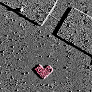
Lovely piece of contamination!
0 com

Welcome back!

After a year (less 3 days), forgetting my password, reseting it, forgetting again, reseting and noting it down in my secret diary... I'm back!

It's been quite a tough year, with lots of new challenges and a little bit of new results!

Now, I promise not to lose the pswd again and be a bit more systematic! In the meantime I offer you two blogs by my colleagues http://thenanolithicera.blogspot.com/ and http://nanoamelia.blogspot.com/ Good reading :)