2 com

Big day coming..


The thesis is done!
After months of writing, deleting, re-writing and re-deleting.... I finally managed to complete my PhD thesis. It's quite a relief to have it done, today the plan is to print it out, put the covers and deliver to the tribunal. The last step is preparing the power point for the defence and by the end of the month I should be a proud doctor in Physics (cross your fingers!!!).
0 com

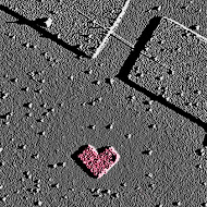
happy st. valentine!

4 com

how to clean graphene?

Graphene is a single layer of carbon atoms. However the problem is that many things like to stick to graphene (polymers, glue from scotch tape, thermal tape, amorphous carbon and all the other kind of  'dirt'). This can be quite dramatic, especially when you realize that sometimes thickness of the dirt accumulated is bigger that the thickness of graphene itself! In that case you have to think, what are you actually measuring? Is it really graphene or graphene + contamination?

To clean graphene a few methods were invented

1. Thermal annealing - annealing in an oven, in high temperature (around 300-350C) and Ar/H2 ambient. All the organic contamination is removed.

2. Current annealing - passing high current through graphene in vacuum. Due to high temperature some of the contamination evaporates and some is moved to the electrodes due to electromigration.

3. Mechanical cleaning - with AFM tip in contact mode. The tip sweeps graphene surface mechanically removing the contamination.

4. Cleaning with carbon nanotubes -  recently I realized that I can use CNTs  to sweep the dirt away from the graphene. If you pass a nanotube on top of graphene surface, it will become very clean and you can easily see it with AFM image. In a way it is similar to AFM contact mode, but it´s much faster: you can sweep 1x1 um in a few seconds.

Below an image of nanotube (MWNT) cleaning graphene:


2 com

70s are back!

Recently I've been really busy with my new devices and hardly getting out of the lab! (everyone now cross their fingers!)
But today I got quite in the party mood with the new image I got with the optical microscope! Shame it's only Wednesday!!


0 com

Italian night out!

To celebrate our group Christmas dinner in an Italian restaurant!


Fantastic pasta, secret family recipe: Cr + Au + HF etching!
0 com

graphene transistor

Hello everyone!

As I was browsing the scientific web today I came across this really nice review of graphene transistors. For everyone who would like to know more about this new invention the link here

The reasons to read it, one by one:

1. It's FOR FREE! (the article, not the transistor)
2. It's in Nature Nano, the best of nano journals
3. graphene transistors are the future of our electronics (or at least we like to believe that..)

Of course some of you may find it too long and too complicated, still it's worth to at least check out the pics ;)

And soon some of MY graphene transistors!
3 com

Salamandra


Feeling a bit fed up with those black-and-white SEM images, today it's time to color up!!!

I'm not so sure if anyone else sees a salamandra in this pic (I do!), in fact it's a leftover of the PMMA layer.
PMMA  is a special kind of resist which we use for electron beam lithography. In this resist we can 'draw' shapes and lines with the electron beam and then fill them with metal, so they stay forever on the chip (like the small cross in the left corner of the pic). The PMMA should go away with acetone, but sometimes it leaves some stains and residues, just like on this sample.


UPDATE! Since nobody else sees a salamandra I propose baboso del mar  (or a sea pancake!)
No. 3 on the list http://de10.com.mx/13048.html  :)