0 com

Polypyrrole

A Nobel prize winner of the year 2000 (among other conductive polymers) in textbook and reality!

(source: Wikipedia)


It has a form of black powder, under the SEM one can see it either as long ribbons or clusters.


Images taken by the author, using Quanta SEM belonging to ICN.
0 com

Earthquake

0 com

Cleanroom Spring/Summer Collection 2013

Today in Extreme Makeover: Cleanroom Edition, especially for the first day of the spring, we have Marianna (28 yo), a lab engineer. Marianna is bored with her usual style and looks for a new, fresh look that will suit her spring mood.

Stylist: This season green is definitely in. It's a great color for blondes, making pale skin and dark eyes more appealing. I went for Talla 2 style, which perfectly fits her frame. The look is completed with classic cleanroom boots. Some may say they are just a cheap Uggs imitation, but this is completely not true. This is a unique design, made of rubber and dust-free material. We gave a it a final touch with a flirty mask, a faint reminiscent of Venice carnival.

Marianna: I'm absolutely amazed! This is probably the best outfit I've ever worn. I would never expect that green all over will make such a good combination. And this mask... I'm loving it!


Before.. (are these boots from the past season?!)


And after! As they say stressed, depressed, but well dressed
0 com

Thesis on-line

For anyone interested my humble thesis in now available online on Tesis Doctorals en Xarxa

I am not particularly proud of it, I'm sure there are various things that could have been done better, but i hope this may help some of you. At least to know which mistakes to avoid! :)
2 com

Why 1D expands on cooling?

If we heat or cool an object we observe a change in its volume. This is due to the thermal expansion, and is described by the thermal expansion coefficient. It describes how the volume changes with temperature.
In the typical 3D solids if we heat up the size of the object will increase (easy!). That behavior is due to increasing of the energy. If we add energy to the system, the vibrations of the lattice atoms become more significant and the average distance between the atoms increases, which in the end contributes to the bigger volume/length of the system. As an easy example think of railway tracks getting deformed during hot, summer days.

Now the situation in 1D and 2D systems is totally different. Measurements were first done on graphene with SEM microscopy and Raman spectroscopy, both of them showing a negative thermal expansion coefficient. That means, that unlike the typical materials graphene contracts with increasing temperature. The negative thermal expansion coefficient was estimated to be rather large 8x 10^-6 1/K.

Then in our work we extracted the thermal expansion coefficient for single-walled carbon nanotubes. Because the nanotubes are so small, and the thermal expansion even smaller, we couldn't measure it directly. Instead we measured the shifts in resonance frequency of a nanotube resonator, which we then related to the change in tension of the nanotube. Taking into account the elongation imposed by contracting gold electrodes and substrate, we could determine the expansion coefficient of a nanotube. This is also negative and relatively large.

What is the reason behind negative thermal expansion of 1 and 2D objects?


This is a simple explanation offered by my ex-boss Adrian Bachtold. At 0 K temperature (so called absolute zero) there are no phonon modes in the sample, so you can imagine it laying completely flat on the surface, with a given length L0. Then if you increase the temperature there are more and more phononic modes, especially the flexural modes which are responsible for deforming the sample. If you then project the length on the sample LT on the surface it will appear shorter.
0 com

Autumn art


We had a few rainy days here last week, clear sign that autumn is coming.
This is one of the autumn-style images, shades of grey and some golden leaves. It respresents a membrane partially destroyed during processing, but if you didn't know it looks like one of the images that can score a high price in Sotheby's!
0 com

Holes and bubbles

Many things have changed recently, I've defended the thesis, went on long holidays, started a new job (http://www.icn.cat/~p2n/) and, well, here I am, back to the lab.
I am mainly working on nano/micro fabrication again, this time trying to develop some suspended SOI structures. There should be no trick in that, but of course something went wrong and the sample seems to be suffering from chicken pox :) We are wishing it a fast recovery!

2 com

Almost a month being a doctor

I'm coming a bit late with updating my status: PhD in Physics (wish it was an option to put it as my status on facebook!), since 29th of June. Below I post some images taken by my Mom.

Panic, panic on the train


With the tribunal.


In a way it's a great relief to manage to defend your thesis, after all the efforts, last-minute corrections and a few panic attacks.My thesis is in general about different electro-mechanical systems made of carbon nanotubes. Electro-mechanical means that the nanotube is set in motion by some kind of electrical stimulation. It can either vibrate like a guitar string (a mechanical resonator) or the electrical force can be used to transport a cargo along the nanotube (a motor). Both types of systems are very interesting, mainly because they behave different than they macro-scale counterparts.
2 com

Big day coming..


The thesis is done!
After months of writing, deleting, re-writing and re-deleting.... I finally managed to complete my PhD thesis. It's quite a relief to have it done, today the plan is to print it out, put the covers and deliver to the tribunal. The last step is preparing the power point for the defence and by the end of the month I should be a proud doctor in Physics (cross your fingers!!!).
0 com

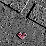
happy st. valentine!

4 com

how to clean graphene?

Graphene is a single layer of carbon atoms. However the problem is that many things like to stick to graphene (polymers, glue from scotch tape, thermal tape, amorphous carbon and all the other kind of  'dirt'). This can be quite dramatic, especially when you realize that sometimes thickness of the dirt accumulated is bigger that the thickness of graphene itself! In that case you have to think, what are you actually measuring? Is it really graphene or graphene + contamination?

To clean graphene a few methods were invented

1. Thermal annealing - annealing in an oven, in high temperature (around 300-350C) and Ar/H2 ambient. All the organic contamination is removed.

2. Current annealing - passing high current through graphene in vacuum. Due to high temperature some of the contamination evaporates and some is moved to the electrodes due to electromigration.

3. Mechanical cleaning - with AFM tip in contact mode. The tip sweeps graphene surface mechanically removing the contamination.

4. Cleaning with carbon nanotubes -  recently I realized that I can use CNTs  to sweep the dirt away from the graphene. If you pass a nanotube on top of graphene surface, it will become very clean and you can easily see it with AFM image. In a way it is similar to AFM contact mode, but it´s much faster: you can sweep 1x1 um in a few seconds.

Below an image of nanotube (MWNT) cleaning graphene:


2 com

70s are back!

Recently I've been really busy with my new devices and hardly getting out of the lab! (everyone now cross their fingers!)
But today I got quite in the party mood with the new image I got with the optical microscope! Shame it's only Wednesday!!


0 com

Italian night out!

To celebrate our group Christmas dinner in an Italian restaurant!


Fantastic pasta, secret family recipe: Cr + Au + HF etching!
0 com

graphene transistor

Hello everyone!

As I was browsing the scientific web today I came across this really nice review of graphene transistors. For everyone who would like to know more about this new invention the link here

The reasons to read it, one by one:

1. It's FOR FREE! (the article, not the transistor)
2. It's in Nature Nano, the best of nano journals
3. graphene transistors are the future of our electronics (or at least we like to believe that..)

Of course some of you may find it too long and too complicated, still it's worth to at least check out the pics ;)

And soon some of MY graphene transistors!
3 com

Salamandra


Feeling a bit fed up with those black-and-white SEM images, today it's time to color up!!!

I'm not so sure if anyone else sees a salamandra in this pic (I do!), in fact it's a leftover of the PMMA layer.
PMMA  is a special kind of resist which we use for electron beam lithography. In this resist we can 'draw' shapes and lines with the electron beam and then fill them with metal, so they stay forever on the chip (like the small cross in the left corner of the pic). The PMMA should go away with acetone, but sometimes it leaves some stains and residues, just like on this sample.


UPDATE! Since nobody else sees a salamandra I propose baboso del mar  (or a sea pancake!)
No. 3 on the list http://de10.com.mx/13048.html  :)
4 com

Silicon Fan


To mark our silicon chips we make a scratch with a diamond tip. Then in the region of the scratch we can sometimes find some pretty structures, just like this one. It reminds a little bit of a Spanish fan, the typical female accessory here, even in 21st century!
4 com

The high frequency resonator finally published!

figureThe good news from last week: the resonator paper is now available online here !


In the paper we measure vibrations of  a very short nanontube, which oscillates with very high frequency - up to 4.2 GHz! That's one of the highest frequencies up to now.


1 com

A bit more about CNT resonators...

Here I show you the image of a high-frequency CNT resonator. It's a suspended SWNT of 100nm length and 4nm diameter.


Now the explication :)
It operates in transistor geometry, as shown below. Source-drain is where the AC current flows, inducing vibrations and with changing voltage on the gate we can change nanotube mechanical tension.
And yes - the actual resonator is the ultra-short carbon nanotube! It's so tiny that it's difficult to image it in SEM. But because it's so small it's easy to achieve high frequency operation!


The details of the high frequency devices will be published in Applied Physics Letters SOON!!! But I'll also try to explain it here in an easier way!
0 com

Carbon nanotube resonators

During this year I worked a on mechanical resonators made of carbon nanotubes.

In general we have two types of carbon nanotubes (CNTs): single-walled (SWNT) and multi-walled (MWNT).  I also put the pictures, for those  who never got the chance to see them before. As the name suggests they are simply very little tubes, but their big advantage for mechanics and electronics is that they are very robust (the most robust material on earth, in fact!) and electrically conductive.


If you want to think of nanotubes for electrical applications, you can consider them as a small cables for nano or micro electrical circuits (easy, they in fact look like small cables) or semiconducting parts of transistor (a bit more difficult).


If you want to think how to apply nanotube mechanical properties, it`s maybe a bit more difficult. One single nanotube is normally too small to be of any use for our world, but is you use big amount of nanotube you can use it to reinforce materials, such as polymers.


Now the last part, think of putting together mechanical and electrical properties of CNTs. One of the options is inducing vibrations of a nanotube (just as you make a guitar string vibrate), but not with mechanical force, but with electric field. (That was exactly the subject of my talk from the previous post!)


Apparently, those little vibrating systems present various interesting properties, quite different from macro-scale. Also resonators made of SWNTs are quite different of those ones made from MWNTs. They can have very good perspective for giga-hertz (GHz) frequency processing and mass sensing.
0 com

My talk in IPN, Mexico, DF

Today I upload a few photos from my recent talk in Instituto Politecnico Nacional in Mexico City, where I came by invitation of  prof. Arturo Borquez.

It was a very exciting moment, first of all because it was my first serious, one-hour talk, but also because I was able to present the results of experiments on carbon nanotube resonators that I was working on during last year!


The announcement! Not yet a PhD, but it felt nice to see the dr title before my name! Of course later I had to explain the misunderstanding..


The introduction


Explaining the importance of nanotechnology


And finally the summary.. Are there any questions???


In the metro, happy with my little reconocimiento :)